Forum Replies Created
-
AuthorPosts
-
 FabrizioModerator
Hello,
the problem is hidden inside your full adder. You must bring your pins (input/output) at the bounding box edge.
In your full adder, the input pins are included in the bounding box making it not possible a direct connecting within the same layer.
Try using the attached one. Remember to replace all the black boxes within the CSA with the new one.Best,
FR
Attachments:
October 23, 2020 at 6:18 am in reply to: Parser Error for synopsys DC generated net list VHDL/.v code in ToPoliNano #2228FabrizioModeratorDear Raja Sekar,
unfortunately feedbacks are not supported in iNML designs.
Best regards.
Fabrizio
FabrizioModeratorDear Rishikesh,
when you apply inputs to the circuit they get inverted on the ANC.
It is normal what you get.Best regards.
FabrizioModeratorDear Rishikesh,
when you apply inputs to the circuit they get inverted on the ANC.
It is normal what you get.Best regards.
November 6, 2019 at 11:02 am in reply to: What is the meaning ofElement translation,function detection …time #1940FabrizioModeratorDear Rishikesh,
Within the log file, the user will find the execution time of the main steps of the VHDL generation algorithm, in particular: element translation, connection detection, and function detection. It is not a problem.
We are updating the documentation to mention also these outputs in the log file.October 23, 2019 at 9:33 am in reply to: magCAD file is closing automatically when i am exporitng the components #1932FabrizioModeratorDear Rishikesh,
we have just released the new version of the tool with the bug fix and some improvement.
FabrizioModeratorHello,
MagCAD doesn’t estimate the power consumption of pNML circuit at the moment. The following discussion can be helpful.
The bounding box area is reported in the .log file produced during the netlist extraction in MagCADFiles->VHDL-><yourcicuit>.
The critical path is reported in the definition file as T_eff, which is the sum of the nucleation time (if available) and propagation time.Best regards.
-
This reply was modified 6 years, 7 months ago by
 Fabrizio.
FabrizioModeratorHi,
I’m happy to hear that you managed to solve this issue. The tool was complaining for a good reason 🙂Regards.
FabrizioModeratorHi,
I suggest you upload the .qll files (if more than one) of your design. Without them, we cannot understand your issue.
Anyway, our emails are within the people section.Regards.
FabrizioModeratorHi,
you are getting the error to the pad in coordinate x=2, y=3 because you cannot connect to another pad. If you look at the documentation you can find the connectivity options for every element. Why would you couple three pads together? Move forward the two pads around the nucleation center and your issue will be solved.
Remember also to assign an output pin to the circuit.Fabrizio
-
This reply was modified 7 years ago by
 Umberto.
FabrizioModeratorHi,
the main power contribution in pNML is related to the switching field required, the clocking circuitry used and the area that should be irradiated. At the moment, it is not integrated into MagCAD. However, you can have a look at the paper “Towards on-chip clocking of perpendicular Nanomagnetic Logic” from M.Becherer which explains a possible solution to clock pNML circuits.
Best.
Fabrizio
FabrizioModeratorHi,
you are getting this error because one of the signals is named “sec”, which is a VHDL keyword for seconds.
Fabrizio
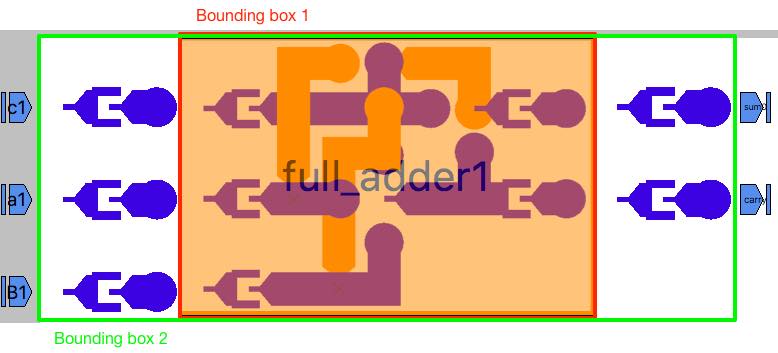
FabrizioModeratorHi,
From your layouts I see that full_adder1 in included in full_adder_box. As a consequence, it is normal the second layout is larger, because you added additional interconnection wires. The bounding box is the minimum box that contains the whole layout.
You con see a summary in the attached picture: bounding_box1 < bounding_box2 as expected.Did you mean something different?
Fabrizio
Attachments:
FabrizioModeratorHi,
I don’t get the point. Can you please upload the .qll files of the 4.18um2 circuit and the 8.1um2?
In general, the circuit latency depends on the critical path, which is represented by the longest nanowire + nucleation. If a component is inserted in a larger design I would expect that the bounding box area increases.Fabrizio
FabrizioModeratorHi Saurabh,
we have updated the documentation with a tutorial on hierarchical designs. This should give the basic information required to achieve a fully working hierarchical circuit.
The hierarchical design is intended to simplify and reduce the complexity of your final architecture re-using existing components.
As happens with every component, the user has to insert the input and output pins also in the top-level circuit, otherwise the VHDL generation cannot be completed.Let me know if documentation can solve your issues.
-
AuthorPosts