
Home › Forums › MagCAD Support › Circuit Design › Use Components in MagCAD
- This topic has 13 replies, 3 voices, and was last updated 7 years, 2 months ago by
 Saurabh Kumar.
-
AuthorPosts
-
February 11, 2019 at 1:10 pm #1676
 Saurabh KumarParticipant
Hi Fabrizio,
Thanks for the help for the previous query.I have another query. I have designed a 4:2 compressor in MagCAD and plan on using it in my multiplier circuit. Is it possible to transform it into a blockm in MagCAD.
Example:-> In Verilog we write the statement
xor x1(sum,a,b,c); where “xor” is a inbuilt function or a block. So is it possible for me to convert my design (4:2 compressor) in a block and use it repeatedly in MagCAD.February 13, 2019 at 11:24 am #1678 UmbertoModerator
Hi Saurabh,
once you designed a circuit you can export it as a component. A component can be used as a black-box in another layout.
Please have a look to the MagCAD documentation for further details.February 19, 2019 at 3:08 pm #1684Saurabh KumarParticipantHi,
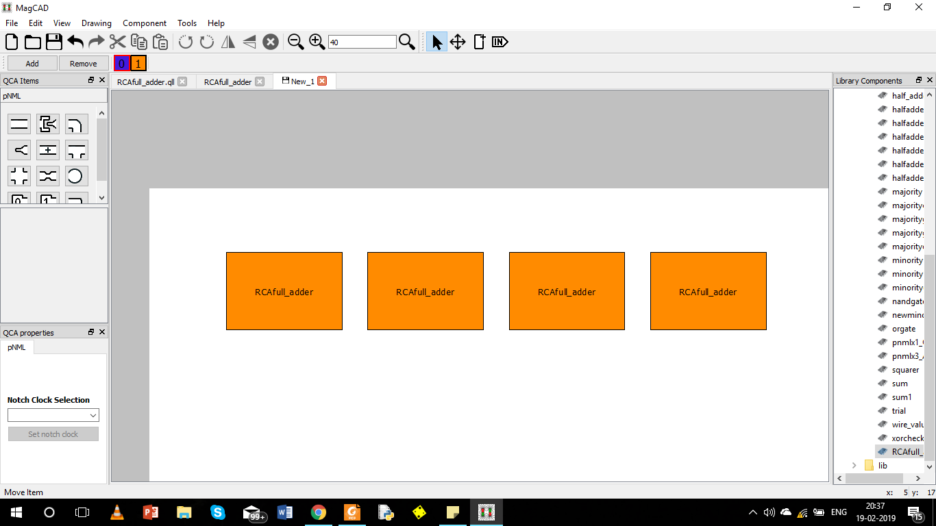
I went through the documentation but couldn’t gather much support from it. I am able to bring 4 full adders( I plan to design 4 bit RCA) but I don’t know how to connect them. I have attached screenshot for that.Also, how will the inputs vary. In the full adder design, the inputs are A, B, and Cin. and this seems to be same for all the adders. In general the inputs are (A0,B0,Cin) then (A1,B1,Carry1) etc.
I request you to please guide me, and if possible, can you make a small video on “how to use a component as black box”.
That would be a great help not just for me but for others as well.Thanks
Attachments:
February 19, 2019 at 3:38 pm #1686Saurabh KumarParticipantI am attaching the QCA file for the full adder and 4 bit RCA file also. full_adder1, full_adder2 etc. are adders I intend to use. Because the limit is 4 files, I couldn’t attach the 4th.
Hope to hear soon from you.Attachments:
February 19, 2019 at 5:22 pm #1691UmbertoModeratorHi Saurabh,
you can use magnets, corners and pads to connect components. Please, consider that it is not needed that you create a different full_adder for each instance: the tool generate different VHDL instances for each full_adder.
Thank you for pointing out this issue. We are updating the documentation with a tutorial for hierarchical designs.
We will update the file ASAP.February 19, 2019 at 5:41 pm #1692Saurabh KumarParticipantHi,
I get that the tool will generate different VHDL automatically. And although I am connecting two adders using magnets, it still shows the error that input is missing.
Another Query is that do the output of one full adder and input for the next full adder should have the same variable name?(In case of RCA.
Please can you demonstrate this using one full adder and implementing a 4-BIT RCA.
Thanks.February 20, 2019 at 9:42 am #1701 FabrizioModerator
Hi Saurabh,
we have updated the documentation with a tutorial on hierarchical designs. This should give the basic information required to achieve a fully working hierarchical circuit.
The hierarchical design is intended to simplify and reduce the complexity of your final architecture re-using existing components.
As happens with every component, the user has to insert the input and output pins also in the top-level circuit, otherwise the VHDL generation cannot be completed.Let me know if documentation can solve your issues.
February 20, 2019 at 12:43 pm #1705Saurabh KumarParticipantHi,
Thanks. IT WORKS!!!!.
Still I feel not satisfied. Reason being, When I use the concept of Black Box and implement, the area and latency increases. If I don’t use the black box concept, the area and latency is reduced.Example an full adder without the black box thing occupies area of 4.18 um2 whereas with the black_box it occupies an area of 8.1um2.
I get the thing that the area will definitely increase because we are adding inputs, wires, and outputs.
But would’t it be better that the area/latency shouldn’t increase. We use the concept of hierarchical method to ease our designing part but if this is at the cost of area and latency, it wouldn’t justify.
OR
when we implement this physically, the area and latency will be reduced (as compared to hierarchical method) irrespective of the design and latency shown in simulation(of hierarchical method) ?
Thanks,
SaurabhFebruary 20, 2019 at 1:22 pm #1706FabrizioModeratorHi,
I don’t get the point. Can you please upload the .qll files of the 4.18um2 circuit and the 8.1um2?
In general, the circuit latency depends on the critical path, which is represented by the longest nanowire + nucleation. If a component is inserted in a larger design I would expect that the bounding box area increases.Fabrizio
February 20, 2019 at 2:32 pm #1707Saurabh KumarParticipantHi. Please find attached the .qll file for both the adders.
Thanks-
This reply was modified 7 years, 2 months ago by Saurabh Kumar.
February 21, 2019 at 7:26 am #1713FabrizioModeratorHi,
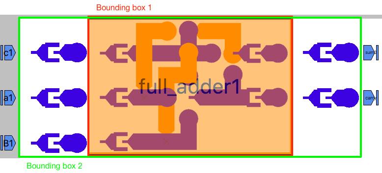
From your layouts I see that full_adder1 in included in full_adder_box. As a consequence, it is normal the second layout is larger, because you added additional interconnection wires. The bounding box is the minimum box that contains the whole layout.
You con see a summary in the attached picture: bounding_box1 < bounding_box2 as expected.Did you mean something different?
Fabrizio
Attachments:
February 21, 2019 at 8:23 am #1715Saurabh KumarParticipantHi,
I get that the area will definitely increase. No doubt at that part. But here what I want to say:The main use of hierarchical method is to reduce circuit complexity without changing its area and latency (Correct me if I am wrong here).
The area will increase because I am adding extra wires, BUT THE LATENCY SHOULD NOT CHANGE WHILE WE USE HIERARCHICAL METHOD while in the above case, the latency also increases while we use the HIERARCHICAL METHOD. I am expecting that the LATENCY SHOULD NOT CHANGE.Is it that when we will use HIERARCHICAL METHOD the latency and area will increase? If yes, then it is better to design the circuit without HIERARCHICAL METHOD because ultimately we want reduced area and delay.
February 21, 2019 at 9:30 am #1716UmbertoModeratorHi,
area and latency are not going to change if you use hierarchical approach or not. Those parameters are related to the circuit design, the number of elements, the functionality and the length of the interconnections in pNML technology. The latency in pNML and in general in NML is the time from an applied input to reach the output. Similarly happens in CMOS: if I design a circuit and then place two of them in series the area and delay will increase, no matter what approach (hierarchical/flat) is used. Indeed, if you use “flat insert” for your fulladder you will get the same values as if you insert it as a component. Obviously, your previous designs are different in area and latency since they are different circuits. I report here the definitions and log files for fulladder_box and the same layout where the component has been replaced with flat elements(see pictures).Fulladder_box | Fulladder_box_flat definitions | definitions -- Entity name: full_adder_box | -- Entity name: full_adder_box_flat -- Element list: | -- Element list: -- Tmagnet 1 | -- Tmagnet 1 -- ------------------- | -- ---------------------- -- via 2 |-- via 2 -- ------------------- |-- ---------------------- -- fa1 1 | -- ------------------- |-- ---------------------- -- corner 5 |-- corner 5 -- ------------------- |-- ---------------------- -- Xmagnet 1 |-- Xmagnet 1 -- ------------------- |-- ---------------------- -- magnet 9 |-- magnet 9 -- ------------------- |-- ---------------------- -- mv3 3 |-- mv3 3 -- ------------------- |-- ---------------------- -- inverter 20 |-- inverter 20 -- ------------------- |-- ---------------------- -- pad 16 | -- pad 16 -- ------------------- |-- ---------------------- log |log Bounding box area: 8.1 um^2. |Bounding box area: 8.1 um^2.As you can see those circuits are identical.
Let me say that those circuits are also useless: if you designed fulladder1 there is no need to design a circuit that instantiates only a fulladder1 and some interconnections. If you want a 2bit rca you need to add two fulladder1 and connect them properly.I hope this solves your issue.
Umberto-
This reply was modified 7 years, 2 months ago by
 Umberto.
-
This reply was modified 7 years, 2 months ago by Umberto.
Attachments:
February 21, 2019 at 3:20 pm #1728Saurabh KumarParticipantYes,
I get it now. The mistake I was doing was, I was comparing the flat design(normal) with the bounding box design.
The design with bounding box will definitely have larger area and latency but that will be equal to the flat design of the bounding box.
Well,
Thank you very much for your continuous support.
Saurabh -
AuthorPosts


- The topic ‘Use Components in MagCAD’ is closed to new replies.