
Currently, the ToPoliNano framework fully supports in-plane Nano Magnetic Logic (iNML) technology. Circuits designed with MagCAD, can be used as custom components in ToPoliNano.
Indeed, the custom circuits can be directly instantiated within the VHDL description.
In addition, automatic-generated layouts generated by ToPoliNano can be re-opened and modified by using MagCAD.
ToPoliNano supported technologies:
- in-plane Nano Magnetic Logic (iNML)
MagCAD supported technologies:
- in-plane Nano Magnetic Logic (iNML)
- perpendicular Nano Magnetic Logic (pNML)
- molecular Field-Coupled Nanocomputing (molFCN)
In the following, a brief description of the three technologies is provided.
iNML
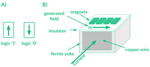
In iNML technology, single-domain nanomagnets are used to represent the binary information. The logic ‘1’ and ‘0’ is encoded in the two stable magnetizations of the
magnet (Fig.1.A), respectively parallel and antiparallel to the easy axis. This is possible due to the shape anisotropy of rectangular magnets. The typical dimensions of a iNML magnet are 90nm x 60nm x 20nm, which represent the height, the width and the thickness respectively. The simplest circuit that it is possible to build is the magnetic wire, obtained cascading an even number of magnets.
The information propagation is obtained thanks to the magneto-dynamic interaction of neighboring magnets. Thus, if the magnetization vector of the input magnet flips, all the other magnets of the wire chain should flip in a domino-like fashion. However this is not true, the shape energy barrier involved in the switch is too high to be won by the dipole-dipole energy supplied by the left magnet. As a consequence, the rest of
the magnets remain stuck and no information propagation happens. To allow the information propagation in iNML, an external agent is required to rotate the magnetization
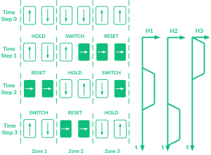
vector of 90°, along the short axis. This external agent, called clock, is the most important element in iNML technology. When the clock field is applied, magnets are forced into an intermediate unstable state (Fig.2). Once the clock is removed, the magnets realign themselves according to the small energy provided by the dipole-dipole interaction. The clock field can be generated placing copper wires under the magnets plane, whereas the field confinement can be obtained using a ferrite yoke (Fig.1.B).
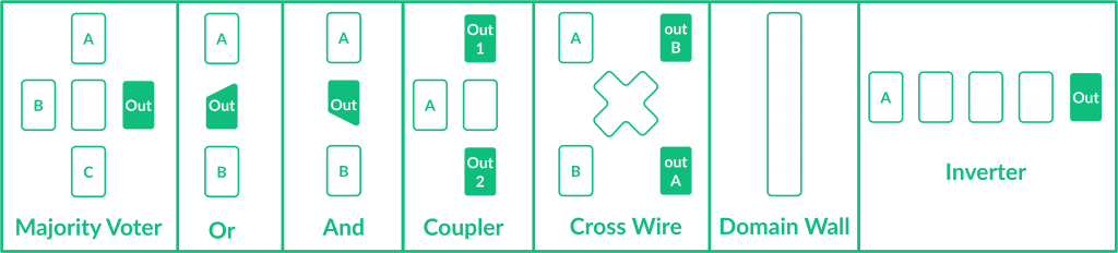
The yoke limits the effects of the magnetic field to a particular zone, the so-called clock zone. On top of that, magnets can be aligned in different ways in order to build magnetic circuits. However, results in the literature show that the number of magnets that can be cascaded above a clocked zone is limited to only 4 or 6 magnets. This is mainly due to the influence of the thermal noise working at room temperature. In literature, several clocking schemes have been proposed to guarantee the correct information propagation in iNML circuits. The clocking scheme implemented in ToPoliNano is based on the 3 partially overlapped phases named Hold, Reset and Switch (Fig.2). The basic gates available in iNML technology are depicted in Fig.3.
For further information please refer to the following references:
[1] F. Riente, G. Turvani, M. Vacca, M. R. Roch, M. Zamboni and M. Graziano, "ToPoliNano: A CAD Tool for Nano Magnetic Logic," in IEEE Transactions on Computer-Aided Design of Integrated Circuits and Systems, vol. 36, no. 7, pp. 1061-1074, July 2017.
[3] Turvani, G. and Riente, F. and Cairo, F. and Vacca, M. and Garlando, U. and Zamboni, M. and Graziano, M., "Efficient and reliable fault analysis methodology for nanomagnetic circuits", International Journal of Circuit Theory and Applications, vol. 45, no.5, 1097-007X, pp. 660-680, 2017.
[2] Wolfgang Porod, Gary H. Bernstein, Gyorgy Csaba, Sharon X. Hu, Joseph Nahas, Michael T. Niemier, and Alexei Orlov., "Field-Coupled Nanocomputing: Paradigms, Progress, and Perspectives", chapter Nanomagnet Logic (NML), pp. 21-32. Springer Berlin Heidelberg, Berlin, Heidelberg, 2014.
[4] G. Csaba, A. Imre, G. H. Bernstein, W. Porod, and V. Metlushko. Nanocomputing by field-coupled nanomagnets. IEEE Transactions on Nanotechnology, 1(4):209-213, Dec 2002.
[5] Csaba, György and Porod, Wolfgang and Csurgay, Árpád I. "A computing architecture composed of field-coupled single domain nanomagnets clocked by magnetic field", International Journal of Circuit Theory and Applications, vol. 31, no. 1, John Wiley & Sons, Ltd., 1097-007X, pag. 67--82, 2003
pNML
The Nano Magnetic Logic implementation that uses magnets with out-of-plane magnetization was proposed by G. Csaba et al. in 2002. Five years later, the NML research group at Lehrstuhl für Technische Elektronik in collaboration with the University of Notre Dame, started the investigation of Cobalt/Platinum (Co/Pt) perpendicularly magnetized magnets. In the subsequent years, the first fully working pNML full adder has been experimentally demonstrated. In the last years, pNML technology has been listed within both the 2014 magnetism roadmap.
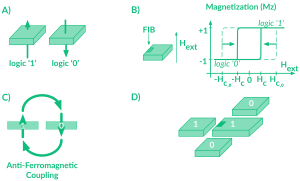
The binary information is encoded in the two stable magnetization state of the magnet. The magnetization up represents the logic ‘1’, whereas the magnetization down the logic ‘0’ (Fig.4.A). The elementary cell is made of a multilayer stack of Co/Pt and it is characterized by a perpendicular magnetic anisotropy (PMA). To define the propagation direction of the information, magnets are FIB irradiated to locally reduce the PMA. This zone is more sensible to the magnetic field variations. Indeed, the switching field in that region is reduced to the coercivity Hc . Basically, what happens is that the hysteresis curve is narrower, as depicted in Fig.4.B. As a consequence, the irradiated side of the magnet is considered as input, i.e. where the domain wall nucleates. In this way, the magnet close to the irradiated spot will influence the switching of the magnet. In general, pNML nanomagnets try to align themselves in an antiparallel or parallel way (Fig. 4.C). The magnetization state of the magnets placed one near the other depends on the anti-ferromagnetic (AF) coupling. However, this technology allows building monolithic 3D devices. When the magnetic information must be transferred from one layer to another, the magnetization state of the magnets depends on the ferromagnetic (F) or AF coupling.
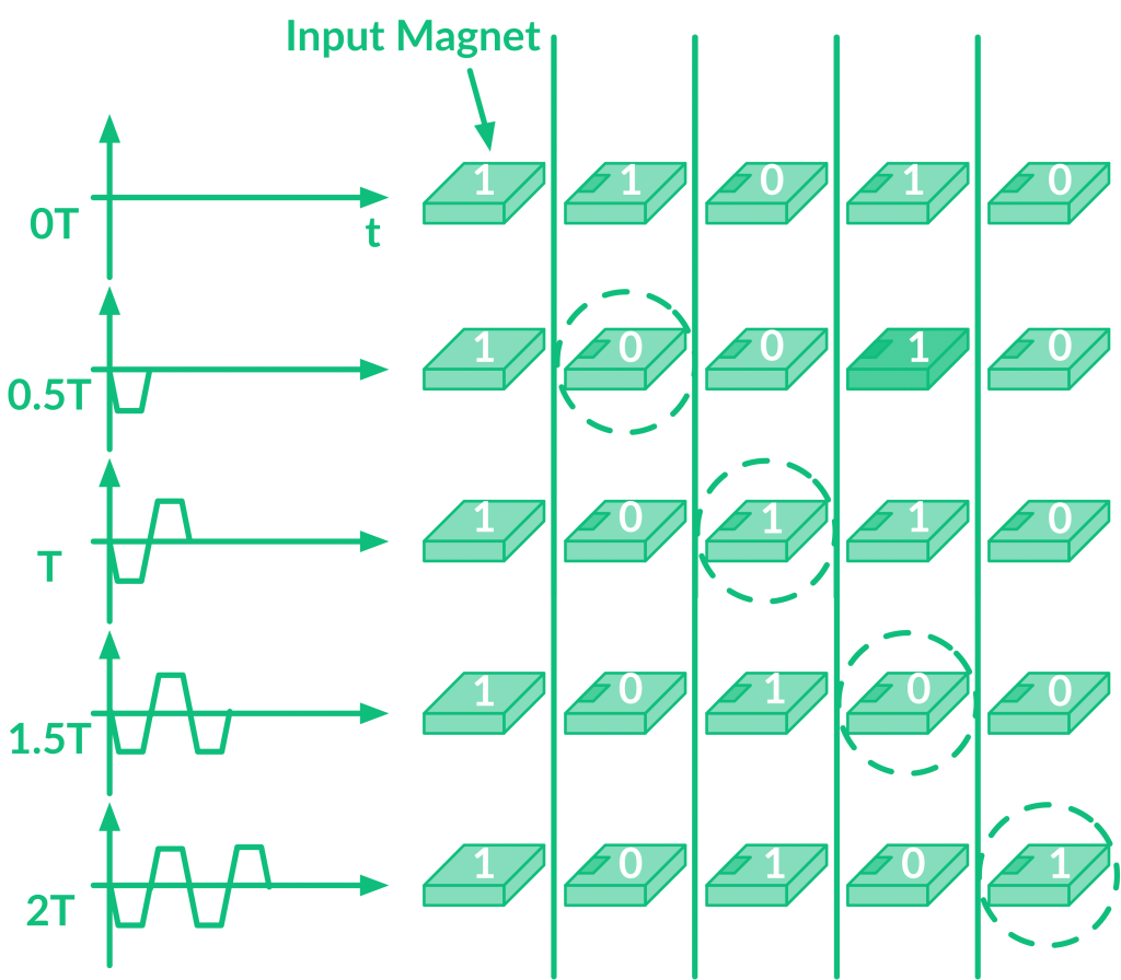
In order to correctly propagate information within the circuit, a perpendicular clock field is required. To better understand how it works, consider the chain of magnets depicted in Fig. 5. Assume that all the magnets have been FIB irradiated on their left side (darker region). At time step 0, there is no clock field applied and the input magnet is magnetized upwards. During the first half clock cycle, a negative field is applied and the magnet close to the input flips its magnetization (AF coupling). When the positive field is applied (1T) the second magnet switches. Now it is clear that the FIB irradiation ensure that the signal propagates from left to right. The clocking field can be considered as an external agent that helps to switch the magnets. The basic computing elements of pNML technology are the inverter and the N-input minority gates (or negated majority). The inverted signal can be easily obtained cascading two nanomagnets. This is just an overview of pNML technology.
For more information please refer to the following references:
[1] Turvani, Giovanna; Riente, Fabrizio; Plozner, Elisa; Vacca, Marco; Graziano, Mariagrazia; Stephan, Breitkreutz-V. Gamm, “A pNML Compact Model Enabling the Exploration of 3D Architectures”. IEEE TRANSACTIONS ON NANOTECHNOLOGY, p. 1. - ISSN 1536-125X. 2017.
[2] F. Riente, G. Ziemys, G. Turvani, D. Schmitt-Landsiedel, S. B. v. Gamm and M. Graziano, "Towards Logic-In-Memory circuits using 3D-integrated Nanomagnetic logic”, 2016 IEEE International Conference on Rebooting Computing (ICRC), San Diego, CA, 2016, pp. 1-8.
[3] Stamps Robert L., Breitkreutz Stephan, Åkerman Johan, Chumak Andrii V., Otani YoshiChika, Bauer Gerrut E. W., Thiele Jan-Ulrich, Bowen Martin, Majetich Sara A., Kl_aui Mathias, Prejbeanu Ioan Lucian, Dieny Bernard, Dempsey Nora M., and Hillebrands Burkard. “The 2014 magnetism roadmap”. Journal of physics Applied physics,  47(33):333001, 2014.
[4] S. Breitkreutz, J. Kiermaier, I. Eichwald, C. Hildbrand, G. Csaba, D. Schmitt-Landsiedel, and M. Becherer. “Experimental demonstration of a 1-bit fulladder in perpendicular nanomagnetic logic”. IEEE Transactions on Magnetics, 49(7):4464-4467, July 2013.
molFCN
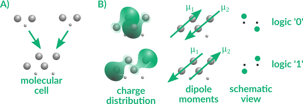
The molecular implementation of Field-Coupled Nanocomputing belongs to the beyond-CMOS world. In this technology, the fundamental elements are specific molecules that can present different charge distributions according to the electric field applied to them. We can build the so-called molecular cell by placing two molecules, one nearby the other (Fig. 6.A). Each cell presents two equivalent minimum-energy configurations where molecules exhibit two opposite dipole moments. The two configurations are assigned to logic values ‘0’ and ‘1’ (Fig. 6.B).
Information propagation and elaboration are obtained through the electrostatic interactions of neighboring cells and the help of the so-called clock electric field that favors or inhibits the correct charge configuration in the cell. Moreover, the presence of the clock field provides a third logic state called NULL state (Fig. 7.A). Indeed, by dividing the circuit into regions controlled by their own clock signal, we can guarantee adiabatic cell switching and pipelined propagation (Fig 7.B).
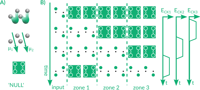
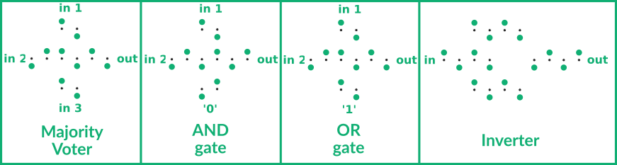
Fig. 8 shows the elementary gates for molFCN. The fundamental gate in this technology is the Majority Voter (MV), whose output equals the logic value present on most of its inputs. From the Majority Voter, it is possible to obtain the 2-inputs AND gate and the 2-inputs OR gate by fixing one input to a logic ‘0’ or a logic ‘1’, respectively.
For further information please refer to the following references:
[1] Lent, C. S., Isaksen, B., & Lieberman, M. (2003). "Molecular quantum-dot cellular automata". Journal of the American Chemical Society, 125(4), 1056-1063.
[2] Ardesi, Y., Pulimeno, A., Graziano, M., Riente, F., & Piccinini, G. (2018). "Effectiveness of molecules for quantum cellular automata as computing devices". Journal of Low Power Electronics and Applications, 8(3), 24.
[3] Ardesi, Y., Beretta, G., Vacca, M., Piccinini, G., & Graziano, M. (2022). "Impact of Molecular Electrostatics on Field-Coupled Nanocomputing and Quantum-Dot Cellular Automata Circuits". Electronics, 11(2), 276.
[4] Pulimeno, A., Graziano, M., Antidormi, A., Wang, R., Zahir, A., & Piccinini, G. (2014). "Understanding a bisferrocene molecular QCA wire". In Field-coupled nanocomputing (pp. 307-338). Springer, Berlin, Heidelberg.
[5] Ardesi, Y., Garlando, U., Riente, F., Beretta, G., Piccinini, G., & Graziano, M. "Taming Molecular Field-Coupling for Nanocomputing Design". ACM Journal on Emerging Technologies in Computing Systems (JETC).