Forum Replies Created
-
AuthorPosts
-
 FabrizioModerator
Dear Chinmay,
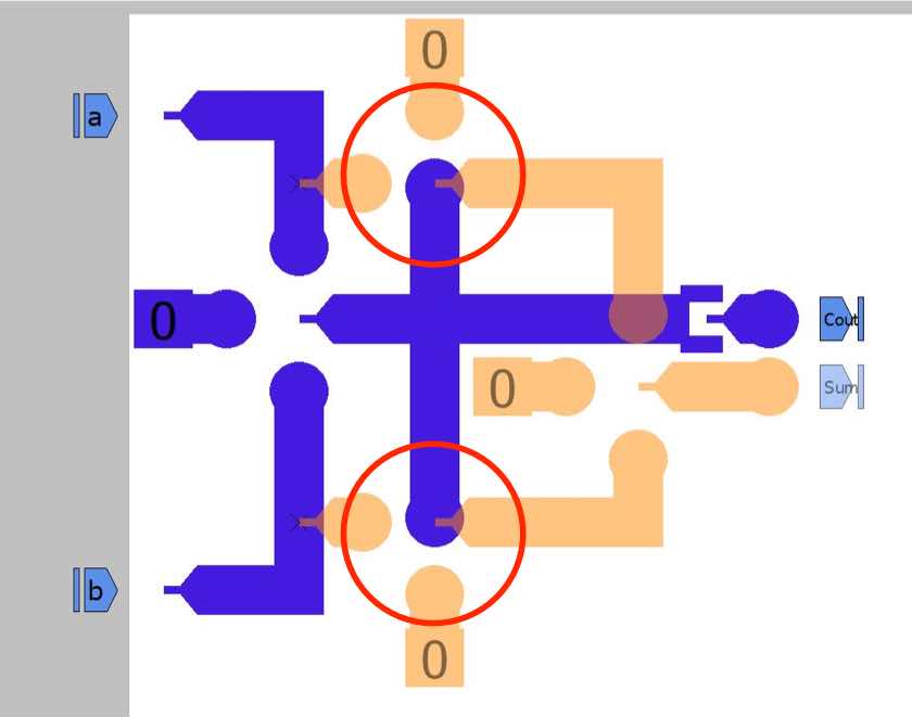
you get a wrong behavior because two gates are not implementing the NAND function (see attachment). When you use 3D gates you should pay attention at the coupling between input magnets and ANC. Magnets lying on the same physical plane are coupled anti-ferromagnetically with ANC. On the contrary, inputs placed above or below the ANC are coupled ferromagnetically.
Please have a look at the following papers:
Attachments:
FabrizioModeratorHi Chinmay,
I think there is an error in the Sum function you are implementing. Try to design it by using only minority in NAND configuration.
Fabrizio
FabrizioModeratorDear Chinmay,
I think that here you have the same problem about the inverted inputs.
Fabrizio
FabrizioModeratorDear Chinmay,
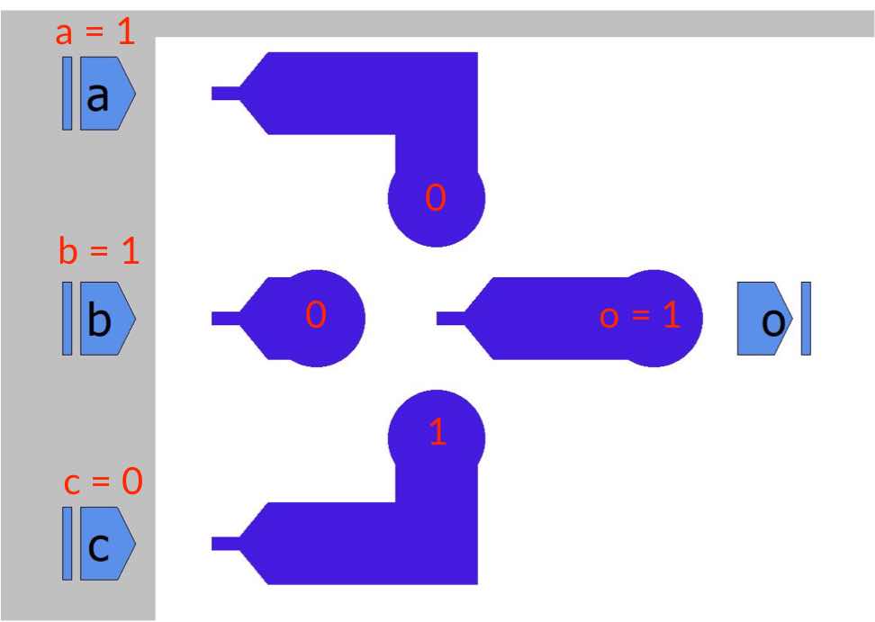
in the MagCAD user guide and in our paper, we consider as input of the minority the magnetisation of the 3 input magnets. Remember that if you apply a 110 within the testbech, you will get a 001 on the input magnets (because you have ANCs which work as inverters). As a consequence, the circuit output will be 1, which is the minority of the inputs. The attached image should clarify your issue.
Let me know if something is still not clear.
Fabrizio
Attachments:
FabrizioModeratorHi Chinmay,
could you please upload the circuit’s layout and a meaningful portion of the waveforms of the 2D minority voter?
Thanks.
Fabrizio
FabrizioModeratorHi Chinmay,
some portions of the generated definition_pnml.vhd are strictly related to the design. As a consequence, you should use the generated “definition” files to simulate your circuit.
The minimum t_clock is automatically computed by the tool during the VHDL netlist extraction, according to the compact model associated to the technology. If you want to change it you can find it within the definition file. Keep in mind that reducing too much t_clock the circuit would not work properly.I hope I have clarified your doubts.
Fabrizio
FabrizioModeratorHi Lavish,
I think that the values you got are a bit different because of the different grid size and the different nanowire width that you used within the design. Please look at the paper and check the parameters used in your design.
The automatic bounding box area calculation will be included in the next release that will be distributed in a few weeks. At the moment you can compute the bounding rectangle by looking at the maximum X and Y coordinate of your design.December 20, 2017 at 2:12 pm in reply to: Optimising the design to implement Boolean expressions #1102FabrizioModeratorYou are right. I was considering the value on the magnets, which is inverted.
December 20, 2017 at 9:43 am in reply to: Optimising the design to implement Boolean expressions #1098FabrizioModeratorHi,
from you screenshots I see two identical gates implementing a 2 input NAND gate. The nucleation center surrounded by 3 inputs implements a negated majority voter.
To optimize circuits, I suggest you to synthetize the boolean network with ABC or by using MIG before drawing the schematics with MagCAD.-
This reply was modified 6 years, 4 months ago by
 Fabrizio.
-
AuthorPosts