
Home › Forums › MagCAD Support › HDL Models › not able to generate VHDL file.
Tagged: pNML
- This topic has 12 replies, 4 voices, and was last updated 7 years, 6 months ago by
 Umberto.
-
AuthorPosts
-
October 31, 2018 at 6:26 pm #1620
 Anshul DalalParticipant
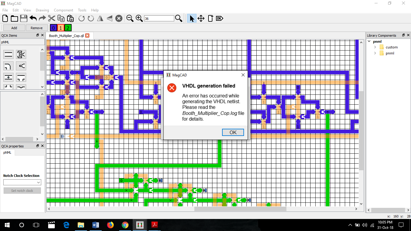
error::
Log of compilation, 31/10/2018 – 22:04:53
Process starts.
2992 VHDL items created.
Output match failed for cell x: 107, y: 34, Layer: 0Checked cell x: 107, y: 34, Layer: 0, but not able to identify the error.
October 31, 2018 at 8:29 pm #1623 FabrizioModerator
Dear Anshul,
as suggested by the pop-up dialog window, you should read the log file generated during the netlist extraction.
The message says that there is a connection problem at x: 107, y:34, layer: 0. Just go with your mouse cursor over the correct coordinate and check if you have properly connected the pNML elements.
For the available connectivity, please have a look at the documentation.In case you still have problem please upload the layout file and not the screenshot.
Best regards.
Fabrizio
-
This reply was modified 7 years, 6 months ago by
 Fabrizio.
November 1, 2018 at 5:06 pm #1625Anshul DalalParticipantThank you for replying.
I am attaching herewith the layout file I am getting error.Attachments:
November 1, 2018 at 5:16 pm #1627Anshul DalalParticipantI had already attached the pdf file in the question too.
I have a couple of doubts too.1. Does MagCAD work fine when working with complex circuit involving more than ‘2’ layers?
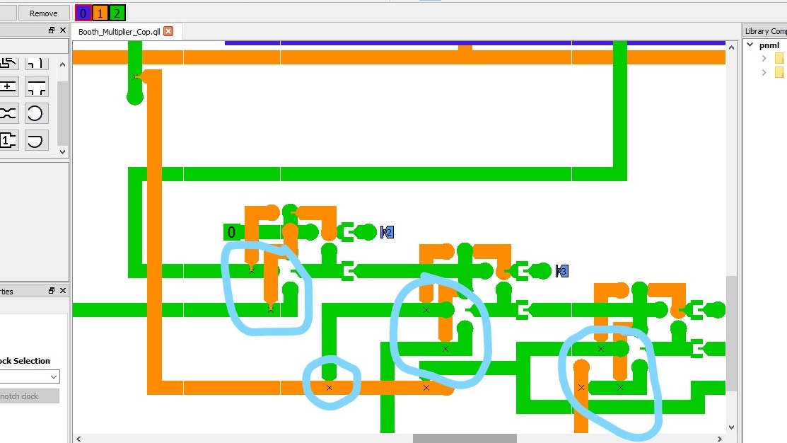
2. Is it valid to take input from an upper layer to the lower layer using ‘Via’ QCA item? I have attached a screenshot below and encircled the cells in which I have used ‘Via’ to take input in a different layer. Please let me know if there is some error in my schematic.
-
This reply was modified 7 years, 6 months ago by Anshul Dalal.
Attachments:
November 1, 2018 at 6:28 pm #1630 UmbertoModerator
Dear Anshul,
you are using the output pin in a wrong way. You have to rotate them by 180°.On the other hand, MagCAD can work with very complex circuits, up to 10000 element on more than 10 layers, so don’t worry 😉
Looking at your screenshot it seems ok.If any error is present the log file will tell you where to look in order to find it.
Best regards,
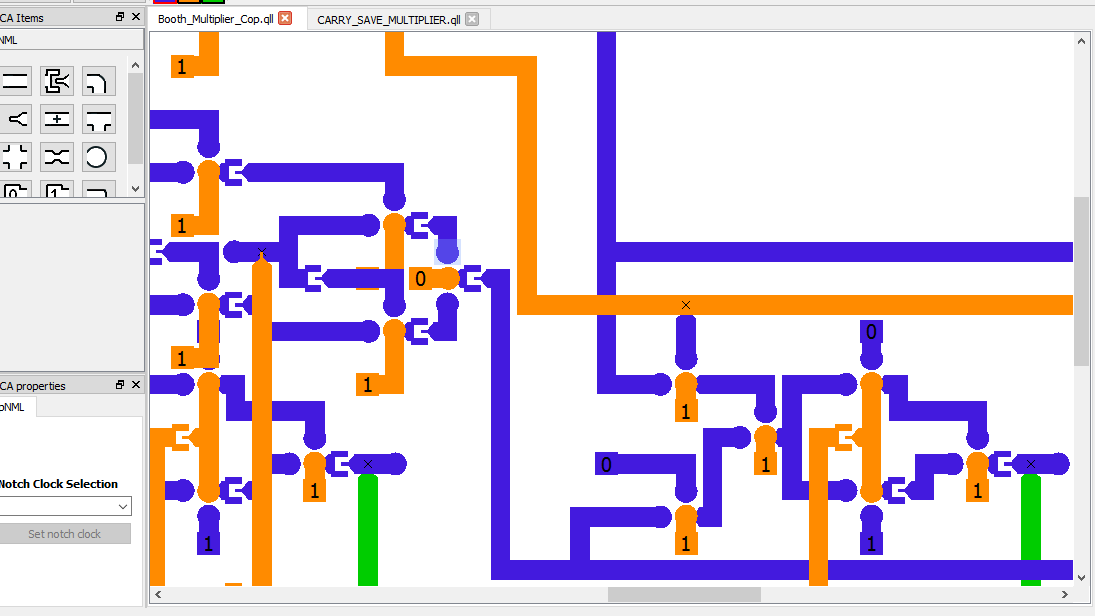
UmbertoNovember 1, 2018 at 7:43 pm #1631Anshul DalalParticipantAs you had pointed, I have flipped the output cell by 180 degrees. But it did not solve the error.
The log file mentioned error at x=132, y=32, layer=0. I deleted the item and placed a new item. Even then I was getting the error at the same coordinates. I’ve also included the error location in screenshot
I closed all files and restarted MagCAD and generated log file for the same schematic. Now the error was at x: 107, y: 34, Layer: 0
I have tried my best to find out the error but nothing appears to be wrong with both these locations.
Attachments:
November 1, 2018 at 7:46 pm #1633Anshul DalalParticipantScreenshot
November 1, 2018 at 9:43 pm #1634UmbertoModeratorDear Anshul,
consider to always attach the qll, it is the best way to see where the problem is.
Going back to your problem, you are connecting a layer 0 via to a layer 3 Nucleation. The coordinates that you can read in the log are the one of the qcc. The layout is always “moved” to the top left corner before generating the qcc and the VHDL.Another problem in your layout, should be just warnings, are the pad unconnected. Consider vias as “T” connection to another plane. If you need just to connect the other layer and terminate the line you can use the pad. The example shows what I’m saying.
Umberto
Attachments:
November 2, 2018 at 2:31 am #1636Anshul DalalParticipantI will make the changes in my layout as per your suggestions and let you know what happens next.
I had already attached the ‘.qll’ file in my earlier post but I’ll post it once again.Attachments:
November 2, 2018 at 5:12 pm #1638UmbertoModeratorDear Anshul,
as I have already told you the error at position 107,34,0 is that you are connecting a layer 0 via to a layer 3 Nucleation.Read my previous post and consider that it is not allowed to pass from layer one to layer 3 without placing a nucleation on layer 2.
Regards,
UmbertoNovember 2, 2018 at 8:31 pm #1639manoj choudharyParticipantSir
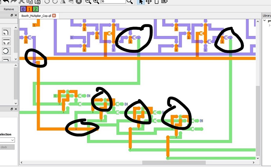
I am making a digital circuit for the project I have been working on
but there is some error in the circuit as vhdl file is not been generatedI checked the cells in the design where error was showing ( in log file) but there is NOTHING WRONG THAT I CAN FIGURE OUT.
Please help!ERROR MESSAGE:
Input missing for cells x: 124, y: 52, Layer: 2
Input missing for cells x: 124, y: 49, Layer: 1
Input missing for cells x: 133, y: 54, Layer: 2
Input missing for cells x: 133, y: 51, Layer: 1
Input missing for cells x: 142, y: 56, Layer: 2
Input missing for cells x: 142, y: 53, Layer: 1Also can we connect layer 0 to layer 2 0r layer 3 directly or do we have to go through layer 1 first.
i have circled the issue in the screenshots and also uploaded .qll fileTHANK YOU
Attachments:
November 2, 2018 at 8:40 pm #1641manoj choudharyParticipantscreenshot
Attachments:
November 3, 2018 at 9:42 am #1645UmbertoModeratorDear Manoj,
your problema is extremely similar to another thread so I will join it.
You could find your answers there.The error is due to the fact that YOU CAN CONNECT ONLY TWO ADJACENT LAYERS.
Regards,
Umberto -
This reply was modified 7 years, 6 months ago by
-
AuthorPosts

- The topic ‘not able to generate VHDL file.’ is closed to new replies.